- 您现在的位置:买卖IC网 > Sheet目录1999 > ICS932S890CKLF (IDT, Integrated Device Technology Inc)IC CLK CHIP EXPRESS 72MLF
932S890C
RD890 SYSTEM CLOCK FOR AMD-BASED SERVERS
IDT
RD890 SYSTEM CLOCK FOR AMD-BASED SERVERS
9
932S890C
REV D 052011
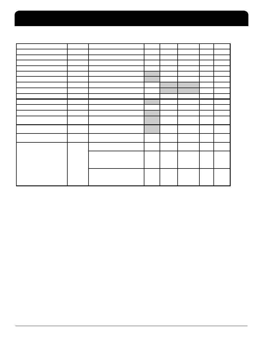
AC Electrical Characteristics–Low-Power DIF Outputs: SRC, SATA
PARA METER
SY MBOL
CONDITIONS
MIN
TYP
MAX
UNITS
NOTES
SRC/S ATA Frequency
fSRC_SATA
Spread Specturm Off
100
MHz
1,6
Long Term Accuracy
p pm
Spread Specturm Off
-50
+50
ppm
1,6
Rising Edge Slew Rate
t
SLR
Differential Measurement
2.5
8
V/ns
1,2
Falling Edge Slew Rate
t
FLR
Differential Measurement
2.5
8
V/ns
1,2
Slew Rate Variation
t
SLVAR
Single-ended Measurement
20
%
1
Maximum Output Voltage
VHIGH
Include s overshoot
1150
mV
1
Minimum Output Voltage
V LOW
Includes undershoot
-300
mV
1
Differential Voltage S wing
V
SWING
Differential Measurement
300
mV
1
Crossing Point Voltage
V
XABS
Single-ended Measurement
300
55 0
mV
1,3,4
Crossing Point Variation
VXABSVAR
Single-ended Measurement
14 0
mV
1,3,5
Duty Cycle
DCYC
Differential Measurement
45
55
%
1
Jitter - Cycle to Cycle
S RCJC2C
Differential Measurement
12 5
ps
1
SRC[13:0] Skew Even Outputs
SRC
SKEW_E
Differential Measurement
20 0
ps
1,8
SRC[13:0] Skew Odd Outputs
SRC
SKEW_O
Differential Measurement
20 0
ps
1,8
SRC[13:0] Even to Odd Skew
SRC
SKEW
Differential Measurement
1275
1375
1475
ps
1,8
P CIe Gen 1 specs
(1.5 - 22 MHz)
40
86
ps
1, 7
PCIe Gen 2 (8-16 MHz, 5-16 MHz)
Lo-band conten t
(10kHz to 1.5MHz)
1.6
3
ps rms
1, 7
PCIe Gen 2 (8-16 MHz, 5-16 MHz)
Hi-band content
(1.5MHz to Nyquist)
2.6
3.1
ps rms
1, 7
1Guaranteed by design and characterization, not 100% tested in production.
2 Slew rate measured through Vswing centered around differential zero
3 Vxabs is defined as the voltage where CLK = CLK#
4 Only applies to the differential rising edge (CLK rising and CLK# falling)
6 All Long Term Accuracy and Clock Period specifications are guaranteed assuming that REFOUT is at 14.31818MHz
Jitter, Phase
tjphaseSRC
5 Defined as the total variation of all crossing voltages of CLK rising and CLK# falling. Matching applies to rising edge rate of
CLK and falling edge of CLK#. It is measured using a +/-75mV window centered on the average cross point where CLK meets
CLK#.
7 Applicable to all SRC outputs. See http://www.pcisig.com for complete specs. Guaranteed by design and characterization, not
tested in production.
8 SRC outputs are divided into two banks, odd and even. The odd bank skew window is 200 ps. The even bank skew window is
200ps. The skew between the even and o dd banks is intentionally set at 1375ps.
发布紧急采购,3分钟左右您将得到回复。
相关PDF资料
ICS93716BGLF
IC DDR PLL CLOCK DRIVER 28-TSSOP
ICS94201DFLF
IC FREQ GENERATOR PROGR 56-SSOP
ICS950218AF
IC TIMING CTRL HUB P4 48-SSOP
ICS950908BFLF
IC TIMING CTRL HUB P4 56-SSOP
ICS951402AGLF
IC TIMING CTRL HUB P4 48-TSSOP
ICS95V847AGIT
IC CLOCK DRIVER 2.5V 24-TSSOP
ICS95V850AGT
IC CLK DVR PLL 1:10 48TSSOP
ICS95V857ALT
IC CLK DVR PLL 1:10 40TVSOP
相关代理商/技术参数
ICS932S890CKLFT
功能描述:IC CLK CHIP EXPRESS 72MLF RoHS:是 类别:集成电路 (IC) >> 时钟/计时 - 专用 系列:- 标准包装:1,500 系列:- 类型:时钟缓冲器/驱动器 PLL:是 主要目的:- 输入:- 输出:- 电路数:- 比率 - 输入:输出:- 差分 - 输入:输出:- 频率 - 最大:- 电源电压:3.3V 工作温度:0°C ~ 70°C 安装类型:表面贴装 封装/外壳:28-SSOP(0.209",5.30mm 宽) 供应商设备封装:28-SSOP 包装:带卷 (TR) 其它名称:93786AFT
ICS932SL901AKLF
制造商:Integrated Device Technology Inc 功能描述:IC ARM SERVER CLOCK 48MLF
ICS932SL901AKLFT
制造商:Integrated Device Technology Inc 功能描述:IC ARM SERVER CLOCK 48MLF
ICS932SQ420BGLF
功能描述:IC CLOCK SYNTHESIZER 64TSSOP RoHS:是 类别:集成电路 (IC) >> 时钟/计时 - 专用 系列:- 标准包装:1,500 系列:- 类型:时钟缓冲器/驱动器 PLL:是 主要目的:- 输入:- 输出:- 电路数:- 比率 - 输入:输出:- 差分 - 输入:输出:- 频率 - 最大:- 电源电压:3.3V 工作温度:0°C ~ 70°C 安装类型:表面贴装 封装/外壳:28-SSOP(0.209",5.30mm 宽) 供应商设备封装:28-SSOP 包装:带卷 (TR) 其它名称:93786AFT
ICS932SQ420DGLF
功能描述:IC CLOCK SYNTHESIZER 64TSSOP RoHS:是 类别:集成电路 (IC) >> 时钟/计时 - 专用 系列:- 标准包装:1 系列:- 类型:时钟/频率发生器,多路复用器 PLL:是 主要目的:存储器,RDRAM 输入:晶体 输出:LVCMOS 电路数:1 比率 - 输入:输出:1:2 差分 - 输入:输出:无/是 频率 - 最大:400MHz 电源电压:3 V ~ 3.6 V 工作温度:0°C ~ 85°C 安装类型:表面贴装 封装/外壳:16-TSSOP(0.173",4.40mm 宽) 供应商设备封装:16-TSSOP 包装:Digi-Reel® 其它名称:296-6719-6
ICS932SQ420DGLFT
制造商:Integrated Device Technology Inc 功能描述:IDTICS932SQ420DGLFT ZERO DELAY FANOUT BU
ICS932SQ420DKLF
功能描述:IC CLOCK SYNTHESIZER 64QFN RoHS:是 类别:集成电路 (IC) >> 时钟/计时 - 专用 系列:- 标准包装:1 系列:- 类型:时钟/频率发生器,多路复用器 PLL:是 主要目的:存储器,RDRAM 输入:晶体 输出:LVCMOS 电路数:1 比率 - 输入:输出:1:2 差分 - 输入:输出:无/是 频率 - 最大:400MHz 电源电压:3 V ~ 3.6 V 工作温度:0°C ~ 85°C 安装类型:表面贴装 封装/外壳:16-TSSOP(0.173",4.40mm 宽) 供应商设备封装:16-TSSOP 包装:Digi-Reel® 其它名称:296-6719-6
ICS932SQ420DKLFT
制造商:Integrated Device Technology Inc 功能描述:IC CLOCK SYNTHESIZER 64-QFP